


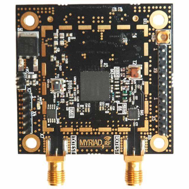
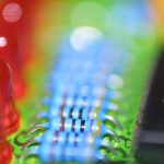
Profound engineering versatility
Imagine being able to rapidly prototype systems of various levels of complexity operating in any wireless standard whether CMDA, WiMax, LTE and HSPA and frequencies of between 300MHz to 3.8GHz using a single RF chip. Well, imagine no more. Lime Microsystems LMS6002D LTD just made that dream come true. Lime’s 5331D3B allows you to do exactly with unmatched ease.
The Field Programmable Radio Frequency
The LMS6002D is one of a kind. It is can be configured to work with any mobile communication frequency. It can also be used with all the three mobile communication standards; 2G, 3G and 4G. Moreover, users can configure the LM66002D to operate with 16 bandwidths up to 28MHz. It embodies a variety of RF inputs and outputs that enable the implementation of multiple features. The 12-bit ADC and DAC built into it allow it to directly connect to any baseband, Digital signal Processing and Field Programmable Gate Array ICs.
The LMS6002D contains standard serial Port Interface (SPI) that are used for programming. It combines LNA, synthesizers, PA driver, RX gain control, RX/TX filters and TX power control. This FPFR replaces individual transceiver chips and allows equipment to be programmed fast and easily. This has led to;
- Reduction in size
- Reduced time to market
- Leaner bill of materials and inventory
The LMS66002D’s fine tuning has led to performance optimization allowing system designers to use fewer components hence reducing the BOM required and the cost incurred.
How it works
The LMSD6002D accepts data as In-phase and Quadrature words. The transmission path then channels this data to a pair of DACs which then convert it into 2 analog signals. However, users could choose to bypass the DACs and apply the signal directly to the device.
The signal then undergoes filtering. LMS66002D’s pass band filter is programmed by users to any of the 16 different bandwidths (1.5-28Hhz). This filtering confines the signal to the selected bandwidth while attenuating any noise out of the selected band.
The pass band filter can also boost the signal by 6dB. The filter is followed by a programmable baseband gain stage which can be configured to offer up to 31dB. The output signal is then mixed so as to achieve the required modulated RF frequency output. The on-board TX PLL synthesizer the input PLL clock by a particular ratio programmed by the user to generate a very stable frequency that has firm accuracy. The RF gain stage, which is also programmable, provides the final signal boost. Without external amplification, the transmit power range is short, approximately tens of meters. To increase this range, external amplifiers will be required.
The LMS6002D’s receiver path is also programmable. It has three LNAs. It also has a general broadband input stage that is designed to handle RF inputs ranging from 300MHz to 3.8GHz. Two LNA’s further enhance the performance of signals ranging between 300 MHz to 2.8GHz (Lo LNA) and 1.5 to 3.8GHz (Hi LNA).
There is a mixer in the receive path that utilizes the same PLL clock as the transmitter. However, it has a different synthesize that provides full duplex and direct down conversion. The signal passes through programmable gain stages and filtering before it finally undergoes digitization then its finally output as I and Q data streams.
The configuration of all the parameters is conducted via a very simple SPI interface into the control logic. Each of the parameters is configured by loading a 16-bit word or on the fly.
Application of the LMS6002
The LMS6002 can be used in a wide range of applications including M2M, communication equipment, SDR and other consumer technologies. Considering its versatility and flexibility, the use of the LMS6002 is only limited to developer’s imagination.
Related posts:
 Ultrasonic Bubbles Detectors and Sensors
 Power Connectors – Ensuring A Secure Electrical Connection
 Top Ten Electronic Machines That Our Kitchen Must Have
 Magnetic Angle Sensor for BLDC Brushless DC Motor
 Modern Electronics Gadgets Where to Buy?
 RGB LED Lighting Shield Board with XMC1202
 Environmental Meter- Multi function Environment Meter
 Bluetooth Low Energy Smart Applications with Bluetooth Mesh
 TE Connectivity USB Type-C Connectors
 What are Benchtop Power Supplies and Their Different Types?
 3D Printing: Formlabs to Shift to Manufacturing
 Circuit Board Development-Enrgtech LTD


