


PCBs
Your phone, laptop, car, TV,and microwave all have one thing in common, they all have printed circuit boards (PCBs). Printed Circuit Board are found in almost every electronic device, they have for a long time formed the foundation of electrical engineering. PCBs are composed of thin layers of conductors “printed” on the surface of an insulating board referred to as the substrate. Individual electronic components are placed on the substrate’s surface and then soldered to the interconnecting circuits. The circuits are connected together by contact fingers running along the edges of the substrate enabling it to connect with the adjacent PCBs or external devices for instance ON/OFF switches.
Printed Circuit Board Composition
A PCB is made up of several alternating layers made from different materials. Their layers are laminated together using heat and adhesives to come up with a single object. These layers are;
- Silkscreen– It is mostly white in color and is usually applied on top of the solder mask. It adds identifiers like letters, symbols,and numbers onto the PCB. These identifiers make it easy to assemble and understand a circuit. They are often used to indicate the function of each pin or LED.
- Solder mask– This is what gives the PCB its green (or sometimes red, purple or white) color. It lies right above the copper layer so that it can insulate the copper traces against unintended contact with good conductors like metals, bits or solder. Solder mask also enables the user to solder on the correct places only while at the same time preventing solder jumps.
- Copper– Right beneath the solder mask is the copper foil. It is can be on a single or both sides of the PCB. PCBs with copper on a single side are however more common than those with copper on both sides.
- Substrate– The substrate forms the base material. It is usually made of fiberglass with the common designator of the fiberglass being FR4. The substrate is solid giving PCBs, their rigidity,and High-temperature plastics like Kapton could also be used to manufacture very flexible PCBs. The thickness of the substrate varies from one PCB to another.
Types of PCBs
There are numerous types of PCB constructions. They include:
- Single-sided– These types of PCBs only have components on a single side of the substrate.
- Double-sided– Can accommodate components on both sides of the board
- Multi-layered– Contains a substrate made up of numerous layers of printed circuits that are separated from each other by insulation.
When double-sided PCBs are used, the electrical connection between the circuits on either side of the PCB is made by drilling holes through the substrate at strategic locations and then plating the holes. The electronic components on the surface of multi-layered PCBs connect via holes made at strategic circuit layer.
Connection of components on PCBs
The electronic components on a PCB are electrically connected to the circuit using two techniques:
Through hole method
In this type of connection, the leads of each component are pushed through small holes drilled in the substrate and then they are soldered to the connection pads contained in the circuit on the opposite side of the PCB.
Surface mount technique
In surface mount technique, the stubby J-shaped or L-shaped legs of each component or placed directly in contact with the circuit. A solder paste made up of glue, flux and solder, is then applied to hold the legs in place until the solder is melted to create the final connection.
Despite demanding a lot of care, surface mount technology eliminates the drilling process which is usually time-consuming. It also saves on the space consumed by the pads in the through hole technique.
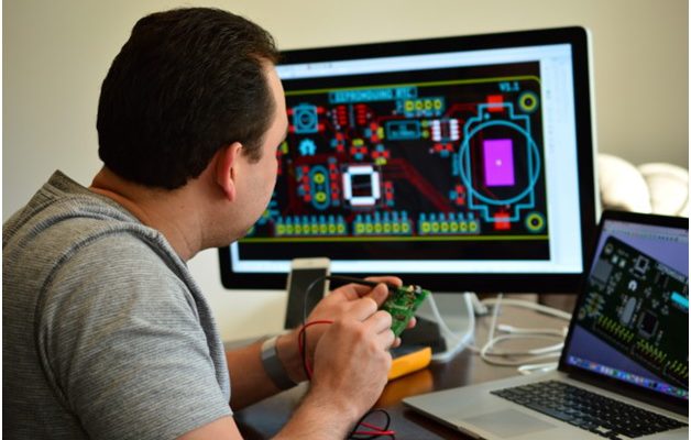
PCB design and development
PCB design largely involves the conversion of a circuit schematic diagram into a PCB layout using software products like Cadsoft Eagle, PCBWizard or Proteus. Printed Circuit Board development firms have machines that perform the printing. However, if you need customized circuits for prototyping or any other use, you can develop it on your own. To do this, you will require the following items:
- Laser printer
- Iron box
- Copper clad laminate
- Etching solution
- Kitchen scrubs
- Thinner
- Plastic coated wire
Step1
Make a printout of your Printed Circuit Board layout using the laser printer. Print the layout on a glossy paper. Remember thatwhat you need is the mirror print out. Print the layout in black and ensure it appears on the glossy side of the paper.
Step2
Cut the copper board to size. You can do this using a cutter or hacksaw. Take the piece you have cut and then rub the copper side. You can use steel wool or sponge scrubs to rub it. Rubbing removes the oxide and the photoresist layers. The rubbed surface allows the image to stick better.
Step3
You now need to transfer the mirror image of the layout to the board. Flip the top layer horizontally and then take the printed side and put it on the rubbed copper surface. It is important to ensure that the board is aligned properly and then tape the printed paper in position.
Alternatively, you can use the circuit as reference to draw a sketch of the layout using a pencil. The moment you are satisfied with it, trace over the sketch with a black marker (permanent).
Step4
Heat up the iron box to the maximum temperature and then iron the printout onto the copper board. To do this efficiently, place the board with the printout still held in position. Hold it firmly using a pliers and then put the hot iron on the other side for a couple of seconds. After that you can now iron the along the printout using the tip of the iron box while applying some pressure onto it for about 15 minutes. The heat from the iron box aids in the transfer of ink on the printout onto the rubbed copper plate. After 15 minutes of ironing, place the board in lukewarm water for about 15 minutes and then remove the paper.
If in the event of removing the paper some of the tracks become faint, you can use a black permanent marker to restore the track.
Step5
The copper board is now ready for etching, butfirst, you need to put on rubber or plastic gloves. Take a plastic container and fill it with water. Dissolve 3 teaspoonfuls of ferric chloride in the water and then dip the PCB into the solution for a half an hour. The solution will react with the unmasked copper hence removing the unwanted copper from the PCB through etching. When ready, use pliers to remove the Printed Circuit Board.
Step 6
Dispose the solution safely. Do not pour it in the sink. Dilute it and dispose it in a sale location. Use thinner to remove the ink from the tracks. Trim the board to its final size and smoothen the edges using a sandpaper. You can then drill the holes and solder your cool components to the board.


